Introduction
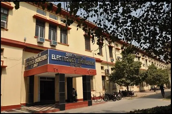
This project proposes the establishment of a state-of-the-art Class-1000 cleanroom facility of 1200 sq. ft. to house sensitive semiconductor fabrication and characterization equipment. The cleanroom will adhere to industry standards for clean environments, ensuring particulate contamination control and optimal conditions for semiconductor device manufacturing and testing.
Estimated Timeline for the Project
12 months
- 6 months for planning and design, and
- 4 months for construction and setup,
- 2 months for testing and training.
Expected Impact
The establishment of a Class-1000 cleanroom is critical for advancing semiconductor research and development within the department. This cleanroom will enable the fabrication of advanced semiconductor devices, particularly those requiring sub-micron precision and low contamination environments. This will open-up the possibility to procure advanced semiconductor fabrication equipment, including a direct laser write lithography system.
This system, with a resolution of 0.6 µm, will significantly enhance our ability to pattern intricate microstructures with high precision, supporting the development of next-generation semiconductor devices. The cleanroom will foster collaborative projects involving academia, industry, and national laboratories, driving forward innovations in semiconductor technologies.
The facility will provide hands-on training for students, researchers, and professionals, offering exposure to the latest fabrication and characterization techniques. This will also help align the department with current trends in semiconductor research, ensuring competitiveness and relevance in the global semiconductor ecosystem.