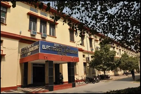
This project proposes the establishment of a state-of-the-art Class-1000 cleanroom facility of 1200 sq. ft. to house sensitive semiconductor fabrication and characterization equipment. The cleanroom will adhere to industry standards for clean environments, ensuring particulate contamination control and optimal conditions for semiconductor device manufacturing and testing.
IIT (BHU) Foundation is an alumni driven endowment fund based in New York, USA to support transformative work being done under infrastructure, research, and education at IIT (BHU).